| CPC H01L 23/3185 (2013.01) [H01L 21/4853 (2013.01); H01L 21/486 (2013.01); H01L 21/565 (2013.01); H01L 23/49827 (2013.01); H01L 23/49838 (2013.01); H01L 23/562 (2013.01); H01L 24/16 (2013.01); H01L 25/0652 (2013.01); H01L 2224/16227 (2013.01); H01L 2924/18161 (2013.01); H01L 2924/3511 (2013.01); H01L 2924/3512 (2013.01)] | 20 Claims |
|
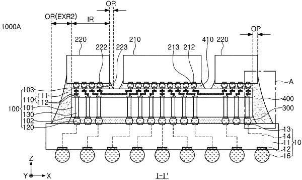
1. A semiconductor package, comprising:
a package substrate;
an interposer disposed on the package substrate;
a first semiconductor chip mounted on the interposer;
a second semiconductor chip mounted on the interposer adjacent to the first semiconductor chip, wherein the second semiconductor chip includes an overhang portion that does not overlap the interposer in a direction perpendicular to an upper surface of the interposer;
a first underfill disposed between the package substrate and the interposer, the first underfill having a first extension portion extending from a side surface of the interposer;
a second underfill disposed between the interposer and the second semiconductor chip, the second underfill having a second extension portion extending to an upper surface of the package substrate along at least a portion of the first extension portion of the first underfill,
wherein the second extension portion covers at least a portion of a side surface of the overhang portion and protrudes from the overhang portion to contact the upper surface of the package substrate.
|