| CPC H01L 23/3185 (2013.01) [H01L 21/563 (2013.01); H01L 21/565 (2013.01); H01L 23/49827 (2013.01); H01L 24/16 (2013.01); H01L 24/73 (2013.01); H01L 25/0655 (2013.01); H01L 25/50 (2013.01); H01L 24/32 (2013.01); H01L 24/81 (2013.01); H01L 24/83 (2013.01); H01L 2224/16227 (2013.01); H01L 2224/32225 (2013.01); H01L 2224/73204 (2013.01); H01L 2224/83855 (2013.01); H01L 2924/3511 (2013.01)] | 18 Claims |
|
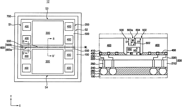
1. A semiconductor package, comprising:
a package substrate;
an interposer provided on the package substrate;
a plurality of semiconductor devices on the interposer to be spaced apart from each other, the semiconductor devices being electrically connected to the package substrate through the interposer;
an underfill member disposed between the plurality of semiconductor devices and the interposer;
a molding layer on the interposer covering at least one side surface of each of the semiconductor devices, covering the underfill member, and exposing upper surfaces of the semiconductor devices, the molding layer including at least one groove extending in a direction separating the semiconductor devices; and
a dummy member arranged on the interposer between the semiconductor devices.
|