| CPC H01L 23/047 (2013.01) [H01L 21/4817 (2013.01); H01L 23/053 (2013.01); H01L 24/29 (2013.01)] | 14 Claims |
|
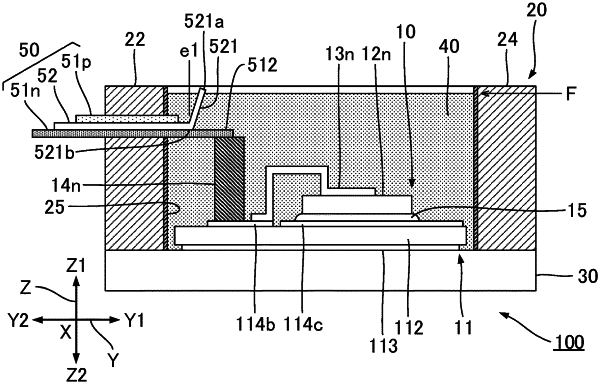
1. A semiconductor module comprising:
a first semiconductor chip including a first main electrode;
a second semiconductor chip including a second main electrode;
a first connection terminal electrically connected to the first main electrode, and including:
a first conductor portion including a first peripheral edge, and
a first terminal portion extending from the first peripheral edge in a plan view of the semiconductor module,
a second connection terminal electrically connected to the second main electrode, and including a second conductor portion including a second peripheral edge; and
an insulating sheet with insulation properties, and including:
an insulating portion layered between the first conductor portion and the second conductor portion, and
a first protruding portion positioned between a tip portion of the first terminal portion and the second peripheral edge in the plan view, the first protruding portion at an angle relative to a surface of the first terminal portion,
wherein
at least a part of the first conductor portion and at least a part of the second conductor portion overlap, one part over an other part, in the plan view.
|