| CPC H01L 22/32 (2013.01) [H01L 21/823814 (2013.01); H01L 21/823821 (2013.01); H01L 21/823878 (2013.01); H01L 27/0924 (2013.01); H01L 29/45 (2013.01)] | 20 Claims |

|
1. A semiconductor device, comprising:
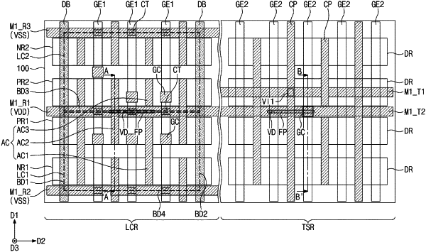
a substrate including a logic cell region and a test region, the logic cell region comprising a first active region and a second active region, which are spaced apart from each other in a first direction, and the test region comprising a plurality of dummy regions, which are spaced apart from each other in the first direction;
a first active pattern and a second active pattern provided on the first active region and the second active region, respectively;
a dummy pattern provided on each of the plurality of dummy regions;
a device isolation layer disposed in a plurality of trenches defining each of the dummy pattern, the first active pattern, and the second active pattern;
a contact pattern provided on the dummy pattern and contacting the dummy pattern;
a first gate electrode provided to cross the plurality of dummy regions and extended in the first direction;
a gate contact coupled to the first gate electrode; and
a first metal layer on the gate contact, wherein the first metal layer is disposed in the logic cell region and the test region,
wherein the first metal layer comprises a first test line and a second test line, which are provided on the test region and are respectively coupled to the contact pattern and the gate contact, and
wherein a top surface of the first active pattern is lower than a top surface of the dummy pattern.
|