| CPC H01L 21/823814 (2013.01) [H01L 21/0259 (2013.01); H01L 21/823807 (2013.01); H01L 21/823878 (2013.01); H01L 27/092 (2013.01); H01L 29/0665 (2013.01); H01L 29/42392 (2013.01); H01L 29/66545 (2013.01); H01L 29/66553 (2013.01); H01L 29/66742 (2013.01); H01L 29/78618 (2013.01); H01L 29/78696 (2013.01)] | 20 Claims |
|
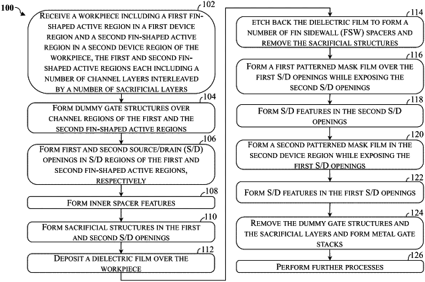
1. A method, comprising:
receiving a workpiece comprising:
a substrate,
an active region protruding from the substrate and comprising a channel region and a source/drain region, and
a dummy gate structure disposed over the channel region;
forming a source/drain trench in the source/drain region of the active region;
forming a sacrificial structure in the source/drain trench;
after the forming of the sacrificial structure, conformally depositing a dielectric film over the workpiece;
performing a first etching process to etch back the dielectric film to form fin sidewall (FSW) spacers extending along sidewalls of the sacrificial structure;
removing the sacrificial structure to expose the source/drain trench;
forming an epitaxial source/drain feature in the source/drain trench, a portion of the epitaxial source/drain feature being sandwiched by the FSW spacers; and
replacing the dummy gate structure with a gate stack.
|