| CPC H01L 21/823431 (2013.01) [H01L 21/823437 (2013.01); H01L 27/105 (2013.01); H01L 28/20 (2013.01); H01L 29/7851 (2013.01)] | 20 Claims |
|
1. A method, comprising:
forming a fin protruding from a substrate;
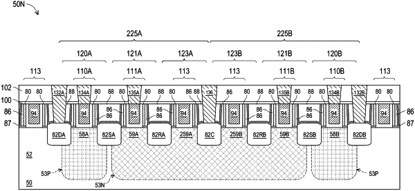
forming a first transistor on the fin, comprising:
forming a first epitaxial drain region and a first epitaxial source region on the fin; and
forming a first gate structure on the fin between the first epitaxial drain region and the first epitaxial source region;
forming a second transistor on the fin, comprising:
forming a second epitaxial drain region and a second epitaxial source region on the fin; and
forming a second gate structure on the fin between the second epitaxial drain region and the second epitaxial source region;
forming a common epitaxial region in the fin between the first epitaxial source region and the second epitaxial source region;
forming a first resistor in the fin between the first epitaxial source region and the common epitaxial region, wherein forming the first resistor comprises implanting a first doped region of the fin that extends from the first epitaxial source region toward the epitaxial common region;
forming a third gate structure on the first doped region of the fin;
forming a second resistor in the fin between the second epitaxial source region and the common epitaxial region, wherein forming the second resistor comprises implanting a second doped region of the fin that extends from the second epitaxial source region toward the epitaxial common region; and
forming a fourth gate structure on the second doped region of the fin.
|