| CPC H01L 21/76865 (2013.01) [H01L 21/32133 (2013.01); H01L 21/32138 (2013.01); H01L 21/76846 (2013.01); H01L 21/76877 (2013.01); H01L 29/401 (2013.01); H10B 10/12 (2023.02); H01L 29/456 (2013.01)] | 15 Claims |
|
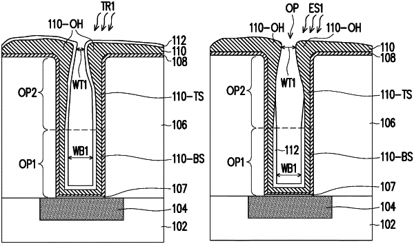
1. A method of fabricating a contact structure, comprising:
forming an opening in a dielectric layer;
forming a conductive material layer within the opening and on the dielectric layer, wherein the conductive material layer comprises a bottom section having a first thickness and a top section having a second thickness, the second thickness is greater than the first thickness;
performing a first treatment on the conductive material layer to form a first oxide layer on the bottom section and on the top section of the conductive material layer; and
performing a second treatment to remove at least portions of the first oxide layer and at least portions of the conductive material layer, wherein after performing the second treatment, the bottom section and the top section of the conductive material layer have substantially equal thickness.
|