US 12,237,214 B2
Method of forming a semiconductor device
Yi-Nien Su, Hsinchu (TW); Shu-Huei Suen, Jhudong Township (TW); Jyu-Horng Shieh, Hsinchu (TW); and Ru-Gun Liu, Zhubei (TW)
Assigned to TAIWAN SEMICONDUCTOR MANUFACTURING COMPANY, LTD., Hsinchu (TW)
Filed by Taiwan Semiconductor Manufacturing Co., Ltd., Hsinchu (TW)
Filed on Jun. 29, 2023, as Appl. No. 18/344,229.
Application 18/344,229 is a continuation of application No. 17/661,600, filed on May 2, 2022, granted, now 11,735,469.
Application 17/661,600 is a continuation of application No. 17/120,989, filed on Dec. 14, 2020, granted, now 11,322,393, issued on May 3, 2022.
Application 17/120,989 is a continuation of application No. 16/525,845, filed on Jul. 30, 2019, granted, now 10,867,840, issued on Dec. 15, 2020.
Claims priority of provisional application 62/737,755, filed on Sep. 27, 2018.
Prior Publication US 2023/0343636 A1, Oct. 26, 2023
Int. Cl. H01L 21/76 (2006.01); H01L 21/02 (2006.01); H01L 21/263 (2006.01); H01L 21/31 (2006.01); H01L 21/311 (2006.01); H01L 21/768 (2006.01)
CPC H01L 21/76802 (2013.01) [H01L 21/02271 (2013.01); H01L 21/02282 (2013.01); H01L 21/2633 (2013.01); H01L 21/31116 (2013.01); H01L 21/31144 (2013.01); H01L 21/76877 (2013.01)] 20 Claims
OG exemplary drawing
 
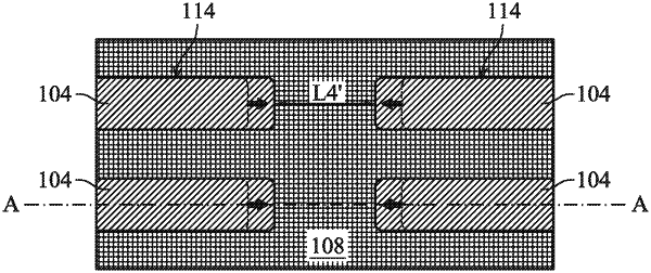
1. A method comprising:
forming a patterned dielectric layer on a substrate;
placing the substrate in a process chamber, wherein the process chamber comprises an aperture assembly and an offset blocking element, wherein a first side of the offset blocking element is separated from the aperture assembly by a first gap, wherein a second side of the offset blocking element is separated from the aperture assembly by a second gap; and
accelerating ions from a plasma generation chamber toward the substrate, wherein ions passing through the first gap etch a first sidewall of the patterned dielectric layer, wherein ions passing through the second gap etch a second sidewall of the patterned dielectric layer.