| CPC H01L 21/76802 (2013.01) [H01L 21/76877 (2013.01); H01L 29/401 (2013.01); G03F 7/094 (2013.01)] | 13 Claims |
|
1. A method for manufacturing a semiconductor device, wherein:
the semiconductor device comprises a substrate and a to-be-connected structure disposed on a side of the substrate; and
the method comprises:
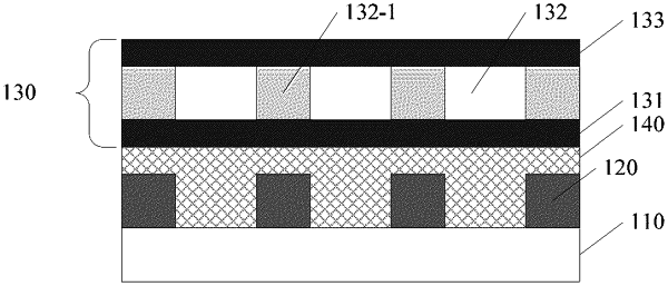
forming a photolithographic coating on the to-be-connected structure, wherein the photolithographic coating comprises a first film, a photolithographic film, and a second film which are stacked in the above-listed sequence, and refractive indexes of the first film and the second film are smaller than 1;
exposing the photolithographic coating to a light having a first wavelength, to image the to-be-connected structure to a first region of the photolithographic film;
exposing the photolithographic coating to a light having a second wavelength through a mask, to image a pattern of the mask to a second region of the photolithographic film; and
forming an electrical connection in contact with the to-be-connected structure at a connection region, wherein the connection region is a region in which the first region and the second region overlap.
|