| CPC H01L 21/76251 (2013.01) [H01L 21/67092 (2013.01)] | 20 Claims |
|
1. A method of forming a semiconductor device, the method comprising:
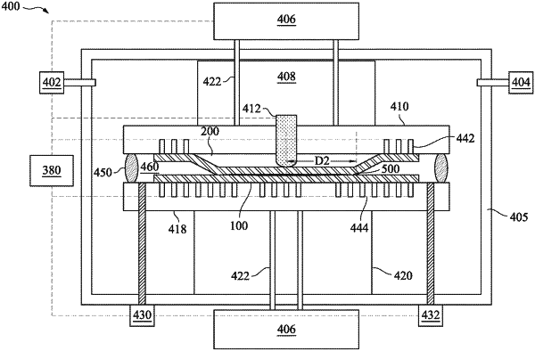
mounting a bottom wafer on a bottom chuck;
mounting a top wafer on a top chuck, wherein a vacuum pressure is applied to at least one of the bottom wafer through the bottom chuck and the top wafer through the top chuck, wherein one of the bottom chuck and the top chuck has a gasket;
moving the top chuck towards the bottom chuck, wherein the gasket forms a sealed region between the bottom chuck and the top chuck around the top wafer and the bottom wafer;
adjusting an ambient pressure in the sealed region, wherein while adjusting the ambient pressure in the sealed region, the vacuum pressure is adjusted to maintain a constant pressure differential between the ambient pressure and the vacuum pressure; and
bonding the top wafer to the bottom wafer.
|