| CPC H01L 21/76229 (2013.01) [H01L 27/0886 (2013.01); H01L 29/0649 (2013.01); H01L 29/7851 (2013.01); H01L 29/7856 (2013.01); H01L 29/78696 (2013.01)] | 18 Claims |

|
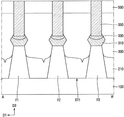
1. A semiconductor device, comprising:
a substrate;
a first fin;
a second fin,
wherein the first and second fins are spaced apart from each other in a first direction on the substrate and extend in a second direction intersecting the first direction;
a first shallow trench formed between the first and second fins;
a field insulating film which fills a first part of the first shallow trench and exposes a second part of the first shallow trench; and
a gate structure on an upper surface of the field insulating film and a part of upper surfaces and side surfaces of the first and second fins, and extending in the first direction,
wherein the gate structure includes a gate electrode and a gate insulating film,
wherein the upper surface of the field insulating film is in a shape of a brace recessed toward the substrate, and has a first point and a second point,
wherein a height from an upper surface of the substrate to the upper surface of the field insulating film is smallest at the first point,
wherein a thickness of the gate insulating film on the first point is different from at least one of a thickness of the gate insulating film on the second point and a thickness of the gate insulating film on the part of the upper surfaces and the side surfaces of the first and second fins, and
wherein a distance from the first point to the first fin in the first direction is different from a distance from the first point to the second fin in the first direction.
|