| CPC H01L 21/76224 (2013.01) [H01L 21/02164 (2013.01); H01L 21/0217 (2013.01); H01L 29/4236 (2013.01); H10B 12/488 (2023.02); H01L 21/311 (2013.01)] | 18 Claims |
|
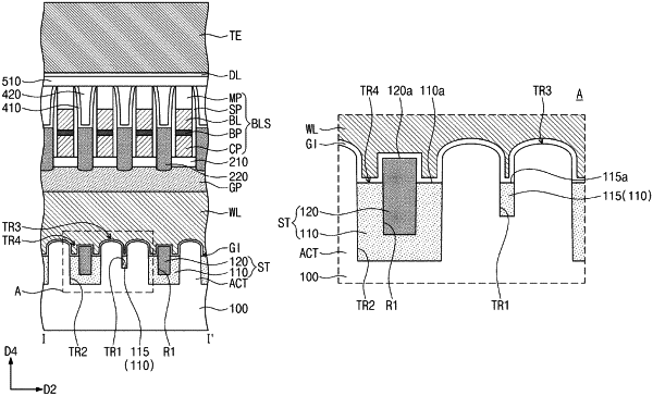
1. A semiconductor device, comprising:
a substrate having one or more inner surfaces defining trenches that define an active pattern of the substrate, the trenches including a first trench and a second trench which have different widths, wherein the substrate has one or more additional inner surfaces that define a third trench penetrating an upper portion of the active pattern;
a device isolation layer on the substrate such that the device isolation layer at least partially fills the trenches, wherein the device isolation layer includes one or more device isolation layer inner surfaces that define a fourth trench penetrating an upper portion of the device isolation layer at least partially filling the second trench; and
a word line intersecting the active pattern,
wherein the device isolation layer includes
a first isolation pattern covering a portion of the second trench,
a second isolation pattern on the first isolation pattern and covering a remaining portion of the second trench, and
a filling pattern filling the first trench under the word line,
wherein a top surface of the second isolation pattern is located at a higher level than a top surface of the filling pattern,
wherein the top surface of the second isolation pattern is located at a lower level than a bottom surface of the third trench and at a higher level than a bottom surface of the fourth trench.
|