| CPC H01L 21/67253 (2013.01) [C23C 16/52 (2013.01); G01B 17/02 (2013.01); G01N 29/041 (2013.01); G01N 29/2443 (2013.01); G01N 29/2462 (2013.01); H01J 37/32963 (2013.01); H01L 21/6719 (2013.01); H01L 22/26 (2013.01); G01N 2291/0231 (2013.01); G01N 2291/02854 (2013.01); G01N 2291/0423 (2013.01); G01N 2291/0426 (2013.01); H01J 2237/24465 (2013.01); H01J 2237/24585 (2013.01); H01J 2237/3321 (2013.01); H01J 2237/334 (2013.01)] | 26 Claims |
|
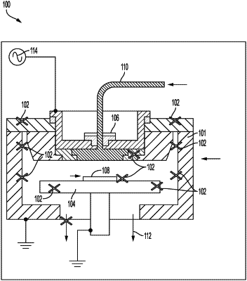
1. A system for monitoring a semiconductor processes, comprising:
a plurality of sensors selectively arranged within a process chamber and configured to issue process signals indicative of a material process occurring proximal to each of the plurality of sensors, the plurality of sensors comprising,
a first sensor defining a first spatial position within the process chamber, and
a second sensor defining a second spatial position within the process chamber, the first spatial position having a different angular orientation than the second spatial position; and,
a microcontroller configured to:
receive the process signals,
correlate the material process sensed by the first and second sensors with a semiconductor process occurring within a current process chamber to acquire information useful for conducting semiconductor processes, and
modify, in real-time, a parameter of the semiconductor process based on the process signals.
|
|
19. A method for monitoring a semiconductor process, the method comprising:
providing a plurality of sensors within a process chamber, the plurality of sensors including,
a first sensor of the plurality of sensors having a first angular orientation and a first position in the process chamber, and
a second sensor of the plurality of sensors having a second angular orientation and second position in the process chamber;
monitoring a deposition or a removal process at different locations within the process chamber;
measuring uniformity of the semiconductor process based on data received from the plurality of sensors during the monitoring step, wherein the first angular orientation and first position of the first sensor and the second angular orientation and second position of the second sensor facilitates measuring the uniformity of the semiconductor processes; and
modifying a parameter of the semiconductor process in real-time based on the data received from the first and second sensor.
|