| CPC H01L 21/31122 (2013.01) [H01L 21/02183 (2013.01); H01L 21/3065 (2013.01)] | 5 Claims |
|
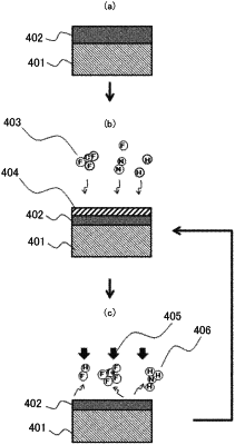
1. An etching method for etching a film layer as a processing object containing nitride of transition metal including tantalum nitride, the film layer being disposed on a surface of a wafer, the method comprising the steps of:
supplying reactive particles containing fluorine and hydrogen but containing no oxygen to a surface of the film layer to form a reaction layer which mainly contains a tantalum-fluorine bond and nitrogen-hydrogen bond and has a self-saturating tendency on the surface of the film layer; and
eliminating the reaction layer by heating the film layer.
|