| CPC H01J 37/32449 (2013.01) [H01J 37/3476 (2013.01); H01L 21/02568 (2013.01); H01L 29/24 (2013.01); H01L 29/242 (2013.01); H01L 29/26 (2013.01); H01L 29/66969 (2013.01); H01L 29/7606 (2013.01); H01L 29/78696 (2013.01); H01J 2237/332 (2013.01); H01J 2237/334 (2013.01); H01L 29/0665 (2013.01); H01L 29/42392 (2013.01)] | 15 Claims |
|
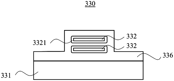
1. A two-dimensional electronic component, comprising:
a substrate;
an artificial two-dimensional (2D) material disposed on the substrate; and
a first metallic electrode disposed on the artificial 2D material;
wherein the artificial 2D material includes a layered atomic structure including a middle atomic layer, a lower atomic layer disposed on a lower surface of the middle atomic layer, and an upper atomic layer disposed on an upper surface of the middle atomic layer respectively; and
wherein the upper atomic layer and the first metallic electrode are attracted together at a junction therebetween by metallic bonding.
|