| CPC H01J 37/32174 (2013.01) [H01J 37/32128 (2013.01); H01J 37/32146 (2013.01); H01J 37/32027 (2013.01); H01J 2237/3341 (2013.01); H01J 2237/3346 (2013.01)] | 19 Claims |
|
1. A method of processing a substrate, comprising performing a processing sequence on the substrate disposed within a processing region of a plasma processing chamber, wherein the processing sequence comprises:
a first process sequence interval that comprises:
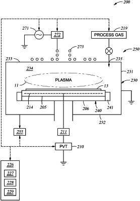
delivering, by a voltage waveform generator, a first burst of first asymmetric voltage pulses to a bias electrode disposed within the plasma processing chamber, wherein the first burst of first asymmetric voltage pulses is provided for a first period of time; and
delivering, by use of a radio frequency (RF) generator, an RF signal to an RF electrode disposed within the plasma processing chamber during the first period of time, wherein the RF signal provided during the first period of time comprises a first RF power level;
a second process sequence interval that comprises:
halting the delivery of the first burst of first asymmetric voltage pulses for a second period of time;
delivering, by use of the RF generator, the RF signal to the RF electrode during the second period of time, wherein the RF signal provided during the second period of time comprises a second RF power level;
a third process sequence interval that comprises:
continuing to halt the delivery of the first burst of first asymmetric voltage pulses for a third period of time; and
halting the delivery of the RF signal to the RF electrode for the third period of time; and
periodically clearing etch by-products during the second process sequence.
|