| CPC G11C 7/222 (2013.01) [G11C 7/1093 (2013.01); G11C 7/1096 (2013.01); G11C 7/225 (2013.01); G11C 11/4076 (2013.01); G11C 11/4093 (2013.01)] | 19 Claims |
|
1. An integrated circuit memory device, comprising:
a memory core;
control logic configured to control the memory core to: (i) output parallel data, and (ii) generate multiple internal clock signals in response to a clock signal received from a host; and
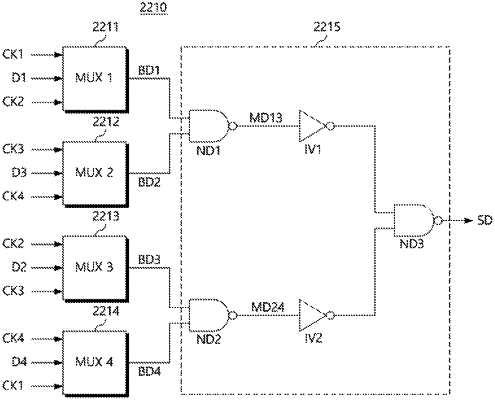
a data transmitting unit including a serializer configured to convert the parallel data into serial data, said serializer comprising:
a plurality of multiplexers that are each configured to output a respective inverted data signal based on one of the parallel data and two of the internal clock signals having different phases relative to each other; and
a serializing circuit configured to output the serial data by logically combining the inverted data signals output from the plurality of multiplexers; and
wherein each of the plurality of multiplexers acquires inverted data of the one of the parallel data between rising edges of the corresponding two internal clock signals and generates therefrom a corresponding one of the inverted data signals.
|