| CPC G11C 7/222 (2013.01) [G11C 7/1039 (2013.01); G11C 7/12 (2013.01); G11C 8/14 (2013.01); H03K 19/01742 (2013.01)] | 20 Claims |
|
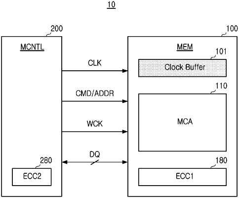
1. A memory device comprising:
a memory cell array having memory cells connected to wordlines and bitlines; and
a clock buffer configured to receive a clock signal for performing a read operation or a write operation on at least one of the memory cells,
wherein the clock buffer includes a plurality of serially connected clock repeaters, and
wherein the plurality of clock repeaters include at least one pair of clock repeaters comprising a first clock repeater in which a driving capability of a P-channel metal oxide semiconductor (PMOS) transistor is higher than a driving capability of an N-channel metal oxide semiconductor (NMOS) transistor, and a second clock repeater in which a driving capability of a PMOS transistor is lower than a driving capability of an NMOS transistor.
|