| CPC G11C 7/1087 (2013.01) [G11C 7/109 (2013.01); G11C 7/1093 (2013.01); G11C 7/222 (2013.01)] | 18 Claims |
|
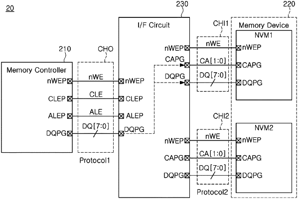
1. A memory system comprising:
first non-volatile memories connected to a first internal channel;
second non-volatile memories connected to a second internal channel;
a memory controller controlling the first and second non-volatile memories through an external channel; and
an interface circuit connecting the external channel to each of the first and second internal channels,
wherein the interface circuit includes:
a command latch enable (CLE) pin, an address latch enable (ALE) pin, and an external data (DQ) pin group, connected to the external channel;
a first command/address (CA) pin group and a first internal DQ pin group connected to the first internal channel;
a decoder configured to determine whether a parallel data signal received from the external DQ pin group is a command signal, an address signal, or a real data signal based on a CLE signal and an ALE signal received from the CLE pin and the ALE pin respectively, and output a decision result signal;
a first serializer configured to serialize the parallel data signal and output the serialized signal to the first internal channel through the first CA pin group;
a first retimer configured to correct a timing of the parallel data signal and output the timing-corrected signal to the first internal channel through the first internal DQ pin group; and
a first demultiplexer configured to provide the parallel data signal to either the first serializer or the first retimer based on the decision result signal of the decoder.
|