| CPC G11C 29/54 (2013.01) [G11C 29/50004 (2013.01)] | 20 Claims |
|
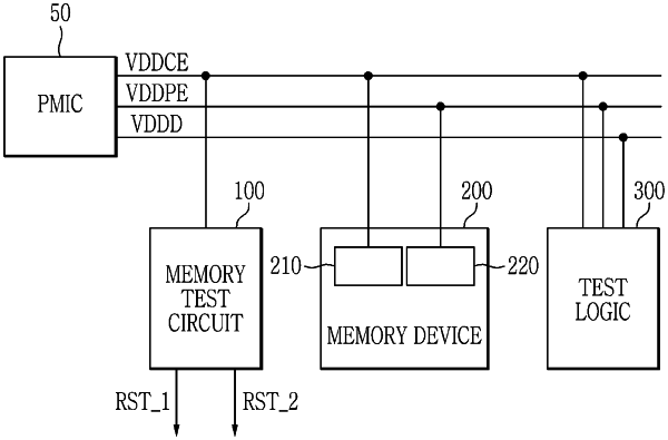
1. A semiconductor device comprising:
a memory test circuit configured to output a fourth signal having a logic level that is based on:
a logic level of a second signal corresponding to a first signal output by a host, and
a logic level of a third signal from a test logic;
a memory device configured to become active or inactive based on the logic level of the fourth signal; and
the test logic, wherein the test logic is configured to:
output the third signal, and
perform a retention test on the memory device based on the logic level of the second signal.
|