US 12,237,030 B2
Layout of driving circuit, semiconductor structure and semiconductor memory
Huijuan Sun, Hefei (CN); and Jihoon Lee, Hefei (CN)
Assigned to CHANGXIN MEMORY TECHNOLOGIES, INC., Hefei (CN)
Filed by CHANGXIN MEMORY TECHNOLOGIES, INC., Hefei (CN)
Filed on Feb. 1, 2023, as Appl. No. 18/162,811.
Application 18/162,811 is a continuation of application No. PCT/CN2021/131909, filed on Nov. 19, 2021.
Claims priority of application No. 202111022398.5 (CN), filed on Sep. 1, 2021.
Prior Publication US 2023/0178164 A1, Jun. 8, 2023
Int. Cl. G11C 29/10 (2006.01)
CPC G11C 29/10 (2013.01) 20 Claims
OG exemplary drawing
 
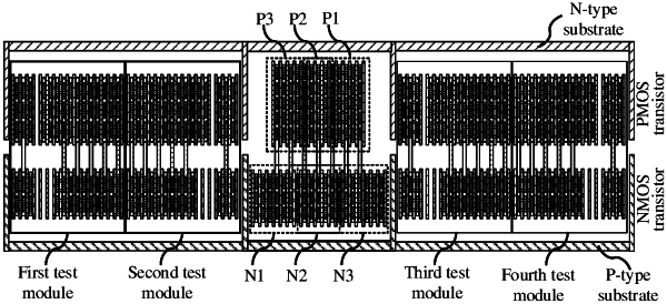
1. A layout of a driving circuit, comprising: P-type transistors, N-type transistors and four test modules, wherein the four test modules are distributed on both sides of the P-type transistors and the N-type transistors in an upper-lower symmetrical structure, and the P-type transistors and the N-type transistors have an upper-lower structure distribution in the middle of the four test modules.