| CPC G11C 16/3445 (2013.01) [G11C 16/08 (2013.01); G11C 16/16 (2013.01); G11C 16/3404 (2013.01)] | 17 Claims |
|
1. A non-volatile memory device, comprising:
a memory including a plurality of blocks; and
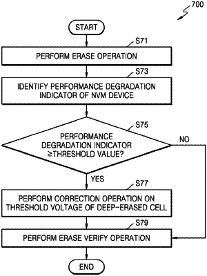
a controller configured to perform an erase operation on at least one block of the memory, perform a correction operation on a threshold voltage of a deep-erased cell among a plurality of cells of the at least one block, and perform an erase verify operation by identifying whether threshold voltages of the plurality of cells fall within a predefined range,
wherein the controller is further configured to, in the correction operation, turn off a string select line and a ground select line of the at least one block and apply a correction voltage to word lines of the at least one block.
|