| CPC G11C 16/26 (2013.01) [G06N 3/063 (2013.01)] | 21 Claims |
|
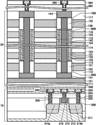
1. A memory device comprising:
a first layer;
a plurality of second layers; and
a third layer,
wherein a first circuit is provided in the first layer,
wherein a first memory cell portion is provided in the plurality of second layers,
wherein a second memory cell portion is provided in the third layer,
wherein the first circuit is configured to drive or control the first memory cell portion and the second memory cell portion,
wherein the first memory cell portion is configured to retain stored data for a longer time than the second memory cell portion, in a state where no power is supplied,
wherein the second memory cell portion is configured to perform data writing and data reading at higher speed than the first memory cell portion,
wherein at least part of the plurality of second layers is stacked over the first layer,
wherein at least part of the third layer is stacked over the plurality of second layers,
wherein the first circuit comprises a first transistor comprising silicon in a channel formation region,
wherein the first memory cell portion comprises a second transistor comprising silicon in a channel formation region,
wherein the second memory cell portion comprises a third transistor comprising a metal oxide in a channel formation region, and
wherein in a cross-sectional view, the second transistor comprises:
a first conductor having an opening portion, the first conductor being configured to be a gate of the second transistor;
a first insulator being in contact with part of a side surface of the opening portion;
a second insulator being in contact with the first insulator in the opening portion;
a third insulator being in contact with the second insulator in the opening portion; and
a semiconductor comprising silicon being in contact with the third insulator in the opening portion, the semiconductor having the channel formation region of the second transistor.
|