| CPC G11C 16/0483 (2013.01) [H01L 23/53266 (2013.01); H01L 23/53295 (2013.01); H10B 41/10 (2023.02); H10B 41/27 (2023.02); H10B 41/35 (2023.02); H10B 43/10 (2023.02); H10B 43/27 (2023.02); H10B 43/35 (2023.02)] | 37 Claims |
|
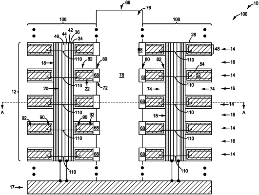
1. An integrated assembly, comprising:
a stack of alternating first and second levels;
a panel extending through the stack; and
the first levels having proximal regions adjacent the panel, and having distal regions further from the panel than the proximal regions; the distal regions comprising conductive structures, with said conductive structures having a first thickness; the proximal regions comprising insulative structures, with said insulative structures having a second thickness at least about as large as the first thickness; and
wherein the second levels comprise void regions between the distal regions of the first levels.
|