| CPC G11C 11/418 (2013.01) [G11C 11/4074 (2013.01); G11C 11/4085 (2013.01); G11C 11/4094 (2013.01); G11C 11/4096 (2013.01); G11C 11/412 (2013.01); G11C 11/419 (2013.01)] | 1 Claim |
|
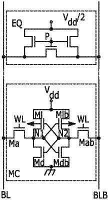
1. A static random-access memory comprising:
a word line circuit for generating a word line signal on a word line:
a plurality of six-transistor memory cells arranged between a first bitline, a second bitline and the word line for simultaneously selecting one of either all or a portion of the plurality of six-transistor memory cells for data reading or writing, and wherein each memory cell comprises:
a first inverter;
a second inverter, the first inverter and the second inverter configured to operate at a power supply voltage (Vdd);
a first n-channel transistor having a gate for receiving the word line signal on the word line and in response connecting a first output of the first inverter to the first bitline;
a second n-channel transistor having a gate for receiving the word line signal on the word line and in response connecting a second output of the second inverter to the second bitline; and
a bitline precharge circuit for precharging the first bitline and second bitline to a voltage of Vdd/2 prior to the first and second n-channel transistors receiving the word line signal, wherein the bitline precharge circuit comprises a first NMOS transistor, a second NMOS transistor and a third NMOS transistor,
wherein a source and a drain of the first NMOS transistor are respectively connected to the first bitline and the second bitline, and a gate of the first NMOS transistor is configured to receive a short signal (ϕshort),
wherein respective drains of the second NMOS transistor and the third NMOS transistor are connected to an output of an on-chip voltage generator,
wherein respective sources of the second NMOS transistor and the third NMOS transistor are respectively connected to the first bitline and the second bitline, and
wherein respective gates of the second NMOS transistor and the third NMOS transistor are configured to receive a precharge signal, ϕprecharge,
wherein, during precharging the first bitline and second bitline, the short signal is turned on before the precharge signal.
|