| CPC G11C 11/4096 (2013.01) [G11C 11/4085 (2013.01); G11C 11/4094 (2013.01)] | 14 Claims |
|
1. A memory device comprising:
a memory cell array including a plurality of memory cells;
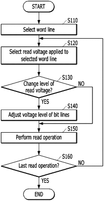
a row control circuit coupled to the memory cells through a plurality of word lines and configured to apply, to a selected word line during read operations, respective read voltages having different levels;
a page buffer circuit coupled to the memory cells through a plurality of bit lines and configured to adjust, according to a sensing control signal during each of the read operations, an amount of current flowing through the bit lines to sense the adjusted amount; and
a read control circuit configured to adjust, during a second read operation subsequent to a first read operation among the read operations, a voltage level of the sensing control signal when a voltage level of a second read voltage corresponding to the second read operation is different from a level of a first read voltage corresponding to the first read operation.
|