| CPC G11C 11/4096 (2013.01) [G11C 11/4087 (2013.01); G11C 11/4091 (2013.01)] | 20 Claims |
|
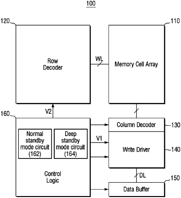
1. A nonvolatile memory device, comprising:
a memory cell array having nonvolatile memory cells therein, which are electrically connected to a plurality of word lines and a plurality of bit lines;
a write driver electrically connected to the plurality of bit lines;
a row decoder electrically connected to the plurality of word lines; and
control logic configured to transfer a first voltage to the write driver and a second voltage to the row decoder, said control logic including: (i) a normal standby mode circuit configured to operate in a normal standby mode, and (ii) a deep standby mode circuit configured to operate in a deep standby mode; and
wherein layout areas of a plurality of elements within the deep standby mode circuit are smaller than layout areas of elements within the normal standby mode circuit, so that current flowing within the deep standby mode circuit during the deep standby mode is less than current flowing within the normal standby mode circuit during the normal standby mode.
|