| CPC G11C 11/4096 (2013.01) [H03K 3/356113 (2013.01)] | 20 Claims |
|
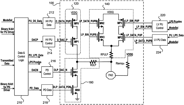
1. An output driver, comprising:
a first pullup driver comprising:
a first PMOS transistor having a source terminal coupled to a first supply voltage and a gate terminal receiving a first data; and
a second PMOS transistor having a source terminal coupled to a drain terminal of the first PMOS transistor and a gate terminal receiving a first analog signal;
a pulldown driver comprising:
a first NMOS transistor having a source terminal coupled to a second supply voltage and a gate terminal receiving a second data different than the first data; and
a second NMOS transistor having a source terminal coupled to a drain terminal of the first NMOS transistor, a drain terminal coupled to a drain terminal of the second PMOS transistor, and a gate terminal receiving a second analog signal; and
a first resistive element coupled between the drain terminal of the second NMOS transistor and a pad of the output driver.
|