| CPC G11C 11/4096 (2013.01) [G11C 11/221 (2013.01); G11C 11/2273 (2013.01); G11C 11/406 (2013.01); G11C 11/4091 (2013.01); G11C 11/4097 (2013.01)] | 20 Claims |
|
1. An apparatus, comprising:
a biasing component configured to:
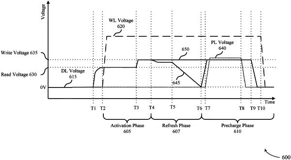
apply a first voltage to a digit line of a memory cell during a first phase of an access operation;
increase the first voltage to a second voltage during the first phase of the access operation;
maintain a third voltage at a plate line of the memory cell for a duration based at least in part on increasing the first voltage to the second voltage; and
initiate a second phase of the access operation based at least in part on a voltage difference between the second voltage and the third voltage.
|