| CPC G11C 11/4091 (2013.01) [G11C 11/4094 (2013.01); G11C 11/4097 (2013.01); G11C 7/06 (2013.01); G11C 7/1048 (2013.01); G11C 2207/002 (2013.01)] | 18 Claims |

|
1. A sense amplifier circuit comprising:
a first bitline;
a first transistor electrically connected between the first bitline and a first node;
a first inverter comprising a first input terminal electrically connected to the first node and a first output terminal;
a second inverter comprising a second input terminal electrically connected to a second node and a second output terminal;
a second transistor comprising a first terminal electrically connected to the first output terminal and a second terminal electrically connected to the second node;
a third transistor comprising a third terminal electrically connected to the second output terminal and a fourth terminal electrically connected to the first node; and
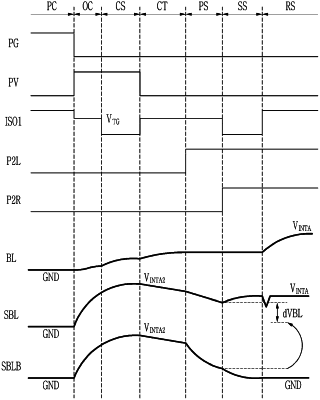
a precharge circuit electrically connected to the first node and the second node, and configured to apply a first voltage to the first node and the second node during a first time period, and apply a second voltage higher than the first voltage to the first node and the second node during a second time period,
wherein a gate of the first transistor is configured to selectively receive a gate voltage from among an enable voltage during precharging of the first bitline by the precharge circuit, a disable voltage when sharing charges between a memory cell and the first bitline, or a bias voltage that is between the enable voltage and the disable voltage when storing offset information of the first transistor.
|