| CPC G11C 11/4085 (2013.01) [G11C 11/4087 (2013.01); G11C 11/4091 (2013.01); H01L 25/0655 (2013.01); H10B 12/482 (2023.02); H10B 12/488 (2023.02); H10B 12/50 (2023.02); H10B 80/00 (2023.02)] | 20 Claims |
|
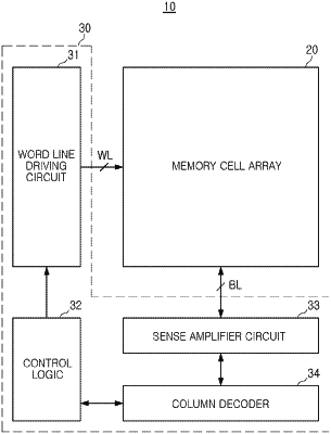
1. A semiconductor device comprising:
a memory cell array that includes a plurality of memory cells electrically connected to a plurality of word lines and a plurality of bit lines;
a word line driving circuit that includes a plurality of sub-word line decoders electrically connected to the plurality of word lines; and
a control logic configured to determine a selected word line and unselected word lines among the plurality of word lines, and configured to control the word line driving circuit such that at least one of the unselected word lines that is adjacent to the selected word line is floated during at least a portion of a period in which a voltage of the selected word line returns to an initial level.
|