| CPC G11C 11/1659 (2013.01) [G11C 11/1675 (2013.01)] | 20 Claims |
|
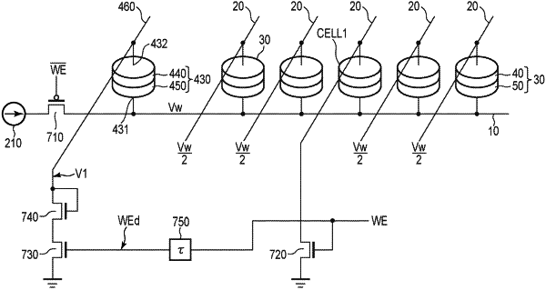
1. A magnetic memory device comprising:
a first wiring line which extends in a first direction;
a plurality of second wiring lines, each of which extends in a second direction intersecting the first direction;
a plurality of first memory cells, each of which includes a first magnetoresistance effect element capable of setting a high resistance state or a low resistance state in which a resistance is lower than a resistance in the high resistance state, and a first selector connected in series to the first magnetoresistance effect element; and
a first switch which includes a first terminal and a second terminal,
wherein
a respective one of the plurality of first memory cells is connected between the first wiring line and a respective one of the plurality of second wiring lines,
the magnetic memory device is configured to apply in operation a first voltage to the second wiring line connected to a selected first memory cell of the plurality of first memory cells, and a second voltage is applied to the second wiring line connected to a non-selected first memory cell of the plurality of first memory cells,
the first terminal of the first switch is connected to the first wiring line, and
the magnetic memory device is configured to apply in operation a third voltage different from the first voltage and the second voltage to the second terminal of the first switch.
|