| CPC G09G 3/3685 (2013.01) [G02F 1/13306 (2013.01); G02F 1/136277 (2013.01); G09G 2310/08 (2013.01); G09G 2330/028 (2013.01)] | 19 Claims |
|
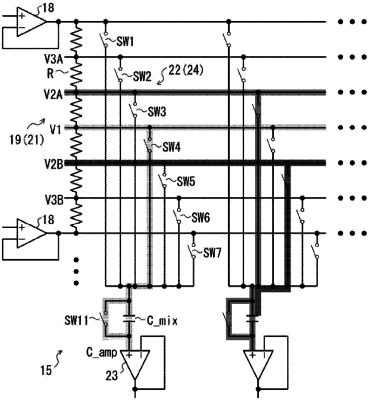
1. A drive circuit, comprising:
a gradation voltage generation unit configured to generate a plurality of gradation voltages that is supplied to a first signal line; and
a voltage selector configured to supply:
a first gradation voltage of the plurality of gradation voltages, to the first signal line, in a first frame period of two consecutive frame periods,
wherein the first gradation voltage has a same voltage level as a specific gradation voltage;
and
a second gradation voltage of the plurality of gradation voltages, to the first signal line, in a second frame period of the two consecutive frame periods,
wherein the second gradation voltage is close to the specific gradation voltage.
|