| CPC G09G 3/36 (2013.01) [G03B 21/006 (2013.01); G03B 21/2073 (2013.01); G09G 3/3614 (2013.01); G09G 2320/0233 (2013.01); G09G 2320/046 (2013.01)] | 15 Claims |
|
15. A drive method, comprising:
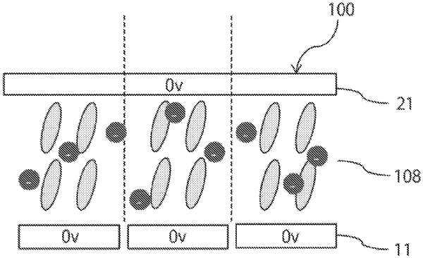
in a display panel having a liquid crystal layer, wherein molecular characteristics of the liquid crystal layer are changed based a potential difference between a first electrode and a second electrode:
outputting a first signal for changing the potential difference based on an input pixel signal;
outputting, as a second signal, at least one of
a signal for changing the potential difference at a predetermined specific cycle, or
a signal for maintaining the potential difference in a direction of reducing ions staying between the first electrode and the second electrode, for a specific time; and
alternately outputting the first signal and the second signal in a turning-on period of light emitted to the liquid crystal layer.
|