| CPC G09G 3/3266 (2013.01) [G09G 3/3291 (2013.01); G11C 19/28 (2013.01); G09G 2310/0202 (2013.01); G09G 2310/0286 (2013.01)] | 20 Claims |
|
1. A display device comprising:
a host system configured to output a timing signal including a clock signal;
a timing controller configured to receive the timing signal and to output gate shift clocks including a first clock signal, a first control clock signal, and a second control clock signal;
a scan driver configured to receive the gate shift clocks and to output scan signals; and
a display unit comprising a plurality of pixels, wherein the scan signals are supplied to the plurality of pixels,
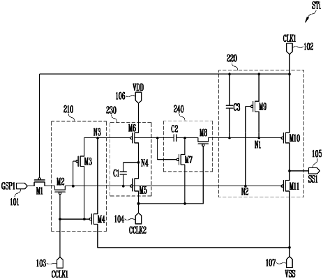
wherein the scan driver comprises:
a first transistor comprising a first electrode and a gate electrode, the first electrode being coupled to a first input terminal, and the gate electrode being coupled to a second input terminal and configured to receive the first clock signal;
an output circuit coupled to the second input terminal and a second power input terminal, and configured to receive the first clock signal such that the output circuit and the gate electrode of the first transistor are both configured to receive the first clock signal, and the output circuit is configured to supply a scan signal to an output terminal in accordance with voltages of a first node and a second node;
an input circuit coupled to a second electrode of the first transistor and to a third input terminal, the third input terminal being configured to receive the first control clock signal, the input circuit being configured to control voltages of the second node and a third node;
a first driving circuit coupled to a first power input terminal and to a fourth input terminal configured to receive the second control clock signal, the first driving circuit being configured to control the voltage of the second node; and
a second driving circuit coupled to the fourth input terminal and the third node, and configured to control the voltage of the first node, and
wherein the first clock signal has a cycle period longer than that of the first control clock signal.
|