| CPC G09G 3/3266 (2013.01) [G09G 2310/0286 (2013.01); G09G 2310/08 (2013.01); G09G 2330/023 (2013.01)] | 20 Claims |
|
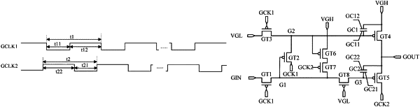
1. A display substrate, comprising a pixel circuit and a scan drive circuit, wherein the pixel circuit comprises a write transistor and a scan signal line electrically connected with a control electrode of the write transistor; and the scan drive circuit comprises a first scan clock signal line and a second scan clock signal line;
a signal of the first scan clock signal line is a first clock signal and a signal of the second scan clock signal line is a second clock signal, both of the first scan clock signal line and the second scan clock signal line are periodic clock signals; and
a duration of the first clock signal being a low-level signal in one period of the first clock signal is different from a duration of the second clock signal being a low-level signal in one period of the second clock signal;
wherein the scan drive circuit comprises N cascaded scan shift registers, wherein each of the scan shift registers receives the first clock signal and the second clock signal.
|