| CPC G09G 3/3233 (2013.01) [G09G 2310/08 (2013.01); G09G 2330/021 (2013.01)] | 8 Claims |

|
1. An electro-optical device comprising:
a first pixel circuit that is provided corresponding to a data line and a first scanning line;
a second pixel circuit that is provided corresponding to the data line and a second scanning line; and
a control circuit that controls the first pixel circuit and the second pixel circuit,
wherein
the first pixel circuit includes
a first light emitting element that emits light with a luminance corresponding to a current flowing between two electrodes, and
a first drive transistor that causes a current corresponding to a voltage between a potential of a gate node and a potential of a source node to flow to the first light emitting element,
the second pixel circuit includes
a second light emitting element that emits light with a luminance corresponding to a current flowing between two electrodes, and
a second drive transistor that causes a current corresponding to a voltage between the potential of the gate node and the potential of the source node to flow to the second light emitting element,
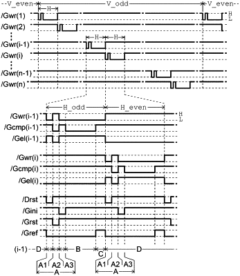
the control circuit, during a first horizontal scanning period in which the first scanning line is selected in a first frame, supplies a potential corresponding to a gradation level to a gate node of the first drive transistor via the data line in a first writing period, and executes a first operation in a first initialization period before the first writing period,
the control circuit, during a second horizontal scanning period in which the second scanning line is selected, supplies a potential corresponding to a gradation level to a gate node of the second drive transistor via the data line in a second writing period, and executes a second operation in a second initialization period before the second writing period,
the first operation is an operation of supplying a first potential to one of the two electrodes via the data line, the first potential being different from a potential corresponding to the gradation level,
the second operation is an operation of setting a potential of the data line and a potential of the one electrode to a potential between the first potential and the second potential, and
the second potential is a potential for setting the first drive transistor and the second drive transistor to be in an OFF state when the second potential is supplied to the gate node.
|