| CPC G09G 3/3233 (2013.01) [G09G 2300/0426 (2013.01); G09G 2300/0819 (2013.01); G09G 2300/0842 (2013.01); G09G 2300/0861 (2013.01); G09G 2320/0233 (2013.01); G09G 2320/045 (2013.01)] | 20 Claims |
|
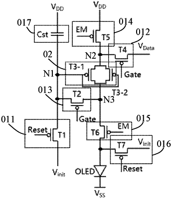
1. A pixel driving circuit, comprising: a light emission control circuit and a drive circuit; wherein
the light emission control circuit is coupled to a gate signal terminal, a data signal terminal, a reset signal terminal, an initial power supply terminal, and a control terminal of the drive circuit, and the light emission control circuit is configured to control a potential of the control terminal of the drive circuit based on a gate driving signal provided by the gate signal terminal, a data signal provided by the data signal terminal, a reset signal provided by the reset signal terminal, and an initial power supply signal provided by the initial power supply terminal; and
an output terminal of the drive circuit is configured to be coupled to a light-emitting element, and the drive circuit is configured to transmit a light emission driving signal to the light-emitting element based on the potential of the control terminal of the drive circuit, to drive the light-emitting element to emit light;
wherein the drive circuit comprises a first drive transistor and a second drive transistor connected in parallel; and a subthreshold swing of one of the first drive transistor and the second drive transistor is greater than a subthreshold swing of the other one of first drive transistor and the second drive transistor.
|