| CPC G09G 3/3233 (2013.01) [G09G 3/32 (2013.01); G09G 3/3275 (2013.01); G09G 2300/0452 (2013.01); G09G 2310/0275 (2013.01); G09G 2320/0233 (2013.01)] | 26 Claims |
|
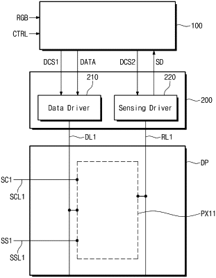
1. A display device comprising:
a display panel including a pixel including a driving transistor and a light-emitting element, and a sensing line connected to the pixel;
a sensing driver which senses a first sensing signal corresponding to mobility of the driving transistor through the sensing line during a sensing period, processes the first sensing signal and outputs first sensing data;
a driving controller which receives the first sensing data from the sensing driver, generates mobility compensation data and kickback compensation data which compensates a kickback voltage generated by a gate-source voltage of the driving transistor based on the first sensing data, and converts image data into compensation image data by the mobility compensation data and the kickback compensation data; and
a data driver which converts the compensation image data into a data signal and provides the data signal to the pixel.
|