| CPC G09G 3/3233 (2013.01) [H10K 59/1201 (2023.02); H10K 59/1213 (2023.02); H10K 59/1216 (2023.02); H10K 59/131 (2023.02); H10K 71/20 (2023.02); H10K 77/111 (2023.02); G09G 2300/0842 (2013.01); G09G 2310/061 (2013.01)] | 19 Claims |
|
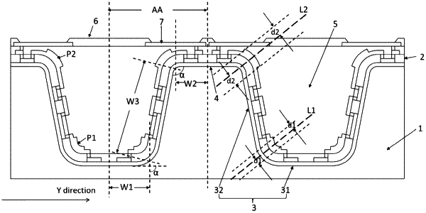
1. A display substrate, comprising a base, and a pixel circuit layer formed on the base, the pixel circuit layer comprises a plurality of pixel driving circuits which are arranged in an array along a first direction and a second direction perpendicular to the first direction, wherein the base has recesses, each of which extends in the first direction and has a bottom surface and a side surface, a surface of the base comprises the bottom surface and the side surface of each of the recesses, and a top surface between adjacent ones of the recesses, the bottom surface of each of the recesses is substantially parallel to the top surface between adjacent ones of the recesses, the side surface of each of the recesses is at a first angle to the bottom surface of the recess and the top surface between adjacent ones of the recesses, and a portion of each of the pixel driving circuits is formed on the side surface of one of the recesses,
wherein each of the pixel driving circuits comprises a driving sub-circuit, a data write sub-circuit, a light emission control sub-circuit, a reset sub-circuit and a storage sub-circuit, the driving sub-circuit, the data write sub-circuit and the storage sub-circuit are formed on the side surface of the recess, the light emission control sub-circuit is formed on the top surface between adjacent ones of the recesses, and the reset sub-circuit are formed on the bottom surface of the recess,
the driving sub-circuit comprises a first transistor, the data write sub-circuit comprises a second transistor and a third transistor, the storage sub-circuit comprises a storage capacitor, the light emission control sub-circuit comprises a fourth transistor and a fifth transistor, and the reset sub-circuit comprises a sixth transistor,
a gate of the first transistor is connected to a first electrode of the second transistor, a first electrode of the storage capacitor, and a first electrode of the sixth transistor, a first electrode of the first transistor is connected to a first electrode of the fourth transistor and a first electrode of the third transistor, and a second electrode of the first transistor is connected to a second electrode of the second transistor and a second electrode of the fifth transistor,
gates of the second transistor and the third transistor each are connected to a scan signal line, a second electrode of the third transistor is connected to a data signal line, and a second electrode of the storage capacitor is connected to a first power supply line,
a second electrode of the fourth transistor is connected to the first power supply line, and gates of the fourth transistor and the fifth transistor each are connected to a light emission control line,
a first electrode of the fifth transistor is connected to an anode of a light-emitting element, and
a gate of the sixth transistor is connected to a reset control line, and a second electrode of the sixth transistor is connected to a reset signal line.
|