| CPC G09G 3/3233 (2013.01) [H10K 50/13 (2023.02); H10K 50/19 (2023.02); H10K 50/852 (2023.02); H10K 59/12 (2023.02); H10K 59/1213 (2023.02); H10K 59/123 (2023.02); H10K 59/131 (2023.02); H10K 59/32 (2023.02); H10K 59/876 (2023.02); G09G 2300/0426 (2013.01); G09G 2300/0842 (2013.01); G09G 2300/0861 (2013.01); G09G 2330/04 (2013.01); H10K 2102/3026 (2023.02)] | 22 Claims |
|
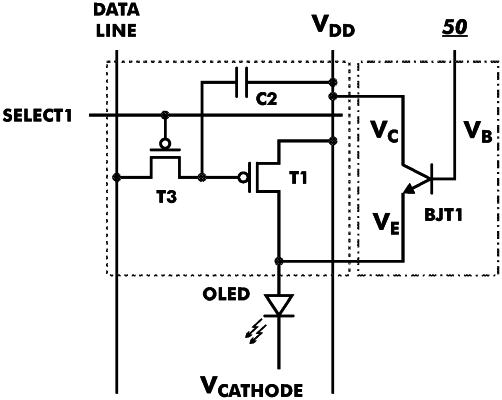
1. A display comprising a light emitting OLED stack on top of a silicon-based backplane with individually addressable pixels and control circuitry wherein:
the control circuitry of the silicon-based backplane comprises at least one driving transistor where a first terminal of the driving transistor is electrically connected to an external power source VDD, and the second terminal of the driving transistor is electrically connected to a segmented bottom electrode of the OLED stack; wherein the gate of the driving transistor is controlled by a data signal which is supplied by a scan transistor controlled by a signal from a first select line; and
the control circuitry additionally comprises a protection circuit comprising a bipolar junction transistor with a collector terminal electrically connected to external power source VDD.
|