| CPC G09G 3/3225 (2013.01) [G09G 2300/02 (2013.01); G09G 2310/0208 (2013.01); G09G 2310/0237 (2013.01); G09G 2310/0286 (2013.01)] | 15 Claims |
|
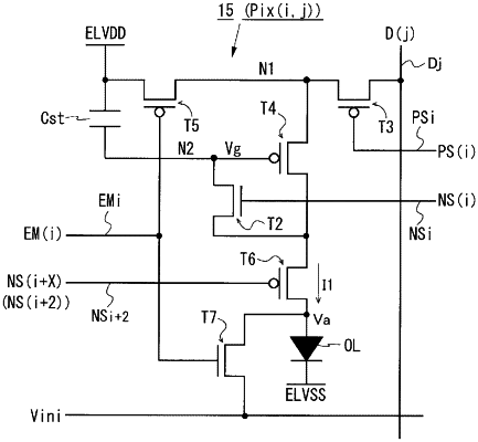
1. A display device, comprising:
a display portion including a plurality of data signal lines, a plurality of first scanning signal lines, a plurality of second scanning signal lines, a plurality of light emission control lines, a first power source line, a second power source line, an initialization voltage line, and a plurality of pixel circuits;
a data-side drive circuit configured to generate a plurality of data signals and apply the generated data signals to the plurality of data signal lines; and
a scanning-side drive circuit configured to selectively drive the plurality of first scanning signal lines, selectively drive the plurality of second scanning signal lines, and selectively deactivate the plurality of light emission control lines,
wherein each of the plurality of pixel circuits
corresponds to one of the plurality of data signal lines, corresponds to one of the plurality of first scanning signal lines, corresponds to one of the plurality of second scanning signal lines, and corresponds to one of the plurality of light emission control lines, and
includes a display element driven by a current, a drive transistor, a holding capacitor, a write control switching element, a threshold compensation switching element, first and second light emission control switching elements whose conductivity types are different from a conductivity type of the threshold compensation switching element, and an initialization switching element whose conductivity type is identical to the conductivity type of the threshold compensation switching element,
the drive transistor has
a first conduction terminal connected to a corresponding data signal line via the write control switching element and connected to the first power source line via the first light emission control switching element,
a second conduction terminal connected to a first terminal of the display element via the second light emission control switching element, and
a control terminal connected to a fixed voltage line via the holding capacitor and connected to the second conduction terminal via the threshold compensation switching element,
the first terminal of the display element is connected to the initialization voltage line via the initialization switching element, and a second terminal of the display element is connected to the second power source line,
the first light emission control switching element has a control terminal connected to a corresponding light emission control line,
the write control switching element has a control terminal connected to a corresponding first scanning signal line,
the threshold compensation switching element has a control terminal connected to a corresponding second scanning signal line,
the initialization switching element has a control terminal connected to the corresponding light emission control line,
the second light emission control switching element has a control terminal connected to a subsequent signal line which is either a subsequent second scanning signal line selected after the corresponding second scanning signal line or a subsequent light emission control line deactivated after the corresponding light emission control line,
the subsequent second scanning signal line is a second scanning signal line that is selected from the plurality of second scanning signal lines such that a select period of the corresponding second scanning signal line overlaps with a select period of the subsequent second scanning signal line,
the subsequent light emission control line is a light emission control that is line selected from the plurality of light emission control lines such that the subsequent light emission control line is deactivated after a start time point of selection of the corresponding second scanning signal line, and such that a select period of the corresponding second scanning signal line overlaps with a select period as a deactivation period of the subsequent light emission control line, and
the scanning-side drive circuit
drives the plurality of first scanning signal lines such that the corresponding first scanning signal line is in a non-select state from the start time point of selection of the corresponding second scanning signal line to a start time point of selection of the subsequent signal line, and is in a select state in an overlapping period of the select period of the corresponding second scanning signal line and the select period of the subsequent signal line, and
selectively deactivates the plurality of light emission control lines such that the corresponding light emission control line is in a deactivated state during the select period of the corresponding second scanning signal line.
|
|
9. A display device, comprising:
a display portion including a plurality of data signal lines, a plurality of first scanning signal lines, a plurality of second scanning signal lines, a plurality of light emission control lines, a first power source line, a second power source line, an initialization voltage line, and a plurality of pixel circuits;
a data-side drive circuit configured to generate a plurality of data signals and apply the generated data signals to the plurality of data signal lines; and
a scanning-side drive circuit configured to selectively drive the plurality of first scanning signal lines, selectively drive the plurality of second scanning signal lines, and selectively deactivate the plurality of light emission control lines,
wherein each of the plurality of pixel circuits
corresponds to one of the plurality of data signal lines, corresponds to one of the plurality of first scanning signal lines, corresponds to one of the plurality of second scanning signal lines, and corresponds to one of the plurality of light emission control lines, and
includes a display element driven by a current, a drive transistor, a holding capacitor, a write control switching element, a threshold compensation switching element, first and second light emission control switching elements, and an initialization switching element,
the drive transistor, the write control switching element, the threshold compensation switching element, the first and second light emission control switching elements, and the initialization switching element are transistors whose conductivity types are all identical,
the drive transistor has
a first conduction terminal connected to a corresponding data signal line via the write control switching element and connected to the first power source line via the first light emission control switching element,
a second conduction terminal connected to a first terminal of the display element via the second light emission control switching element, and
a control terminal connected to a fixed voltage line via the holding capacitor and connected to the second conduction terminal via the threshold compensation switching element,
the first terminal of the display element is connected to the initialization voltage line via the initialization switching element, and a second terminal of the display element is connected to the second power source line,
the first light emission control switching element has a control terminal connected to a corresponding light emission control line,
the write control switching element has a control terminal connected to a corresponding first scanning signal line,
the threshold compensation switching element has a control terminal connected to a corresponding second scanning signal line,
the initialization switching element has a control terminal connected to the corresponding second scanning signal line,
the second light emission control switching element has a control terminal connected to a subsequent light emission control line that is deactivated after the corresponding light emission control line is deactivated,
the subsequent light emission control line is a light emission control line that is selected from the plurality of light emission control lines such that the subsequent light emission control line is deactivated after a start time point of selection of the corresponding second scanning signal line, and such that a select period of the corresponding second scanning signal line overlaps with a select period as a deactivation period of the subsequent light emission control line, and
the scanning-side drive circuit
drives the plurality of first scanning signal lines such that the corresponding first scanning signal line is in a non-select state from the start time point of selection of the corresponding second scanning signal line to a start time point of deactivation of the subsequent light emission control line, and is in a select state in an overlapping period of the select period of the corresponding second scanning signal line and the select period of the subsequent light emission control line, and
selectively deactivates the plurality of light emission control lines such that the corresponding light emission control line is in a deactivated state during the select period of the corresponding second scanning signal line.
|
|
13. A drive method of a display device using a display element driven by a current,
wherein the display device includes a display portion including a plurality of data signal lines, a plurality of first scanning signal lines, a plurality of second scanning signal lines, a plurality of light emission control lines, a first power source line, a second power source line, an initialization voltage line, and a plurality of pixel circuits,
each of the plurality of pixel circuits
corresponds to one of the plurality of data signal lines, corresponds to one of the plurality of first scanning signal lines, corresponds to one of the plurality of second scanning signal lines, and corresponds to one of the plurality of light emission control lines, and
includes a display element driven by a current, a drive transistor, a holding capacitor, a write control switching element, a threshold compensation switching element, first and second light emission control switching elements whose conductivity types are different from a conductivity type of the threshold compensation switching element, and an initialization switching element whose conductivity type is identical to the conductivity type of the threshold compensation switching element,
the drive transistor has
a first conduction terminal connected to a corresponding data signal line via the write control switching element and connected to the first power source line via the first light emission control switching element,
a second conduction terminal connected to a first terminal of the display element via the second light emission control switching element, and
a control terminal connected to a fixed voltage line via the holding capacitor and connected to the second conduction terminal via the threshold compensation switching element,
the first terminal of the display element is connected to the initialization voltage line via the initialization switching element, and a second terminal of the display element is connected to the second power source line,
the first light emission control switching element has a control terminal connected to a corresponding light emission control line,
the write control switching element has a control terminal connected to a corresponding first scanning signal line,
the threshold compensation switching element has a control terminal connected to a corresponding second scanning signal line,
the initialization switching element has a control terminal connected to the corresponding light emission control line,
the second light emission control switching element has a control terminal connected to a subsequent signal line which is either a subsequent second scanning signal line selected after the corresponding second scanning signal line or a subsequent light emission control line deactivated after the corresponding light emission control line,
the subsequent second scanning signal line is a second scanning signal line that is selected from the plurality of second scanning signal lines such that a select period of the corresponding second scanning signal line overlaps with a select period of the subsequent second scanning signal line,
the subsequent light emission control line is a light emission control line that is selected from the plurality of light emission control lines such that the subsequent light emission control line is deactivated after a start time point of selection of the corresponding second scanning signal line, and such that a select period of the corresponding second scanning signal line overlaps with a select period as a deactivation period of the subsequent light emission control line, and
the drive method includes
driving the plurality of first scanning signal lines such that the corresponding first scanning signal line is in a non-select state from the start time point of selection of the corresponding second scanning signal line to a start time point of selection of the subsequent signal line, and is in a select state in an overlapping period of the select period of the corresponding second scanning signal line and the select period of the subsequent signal line, and
selectively deactivating the plurality of light emission control lines such that the corresponding light emission control line is in a deactivated state during the select period of the corresponding second scanning signal line.
|