| CPC G09G 3/3225 (2013.01) [G09G 3/002 (2013.01); G09G 2300/02 (2013.01); G09G 2300/0426 (2013.01); G09G 2300/0452 (2013.01); G09G 2320/0626 (2013.01)] | 19 Claims |
|
1. A display substrate, comprising:
a base substrate, comprising a first display region and a second display region on at least one side of the first display region, wherein a light transmittance of the first display region is greater than that of the second display region; and
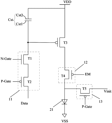
a plurality of first sub-pixels on the base substrate and in the first display region, wherein at least one of the plurality of first sub-pixels comprises: a first pixel circuit and a first light emitting device, and the first pixel circuit comprises: a storage capacitor and a driving transistor; a first electrode of the driving transistor is connected to a first voltage line; and two plates of the storage capacitor are connected to a gate electrode and the first electrode of the driving transistor, respectively;
the first pixel circuit further comprises:
a data writing sub-circuit configured to write a data voltage signal to the gate electrode of the driving transistor in response to a first scan signal and a second scan signal;
a reset sub-circuit configured to provide an initialization voltage signal to a first electrode of the first light emitting device in response to the second scan signal; and
a luminescent control sub-circuit configured to transmit a driving current output from the driving transistor to the first light emitting device in response to a luminescent control signal; and
wherein an orthographic projection of the first electrode of the first light emitting device on the base substrate covers at least a part of an orthographic projection of the first pixel circuit on the base substrate; and
wherein the data writing sub-circuit comprises:
a first writing transistor, wherein a gate electrode of the first writing transistor is connected to a first scan line for providing the first scan signal, a second electrode of the first writing transistor is connected to the gate electrode of the driving transistor, and the first writing transistor is an oxide transistor; and
a second writing transistor, wherein a gate electrode of the second writing transistor is connected to a second scan line for providing the second scan signal, a first electrode of the second writing transistor is connected to a data line for providing the data voltage signal, a second electrode of the second writing transistor is connected to a first electrode of the first writing transistor, and the second writing transistor is a polysilicon transistor.
|