| CPC G09G 3/3208 (2013.01) [G09G 2300/0426 (2013.01); G09G 2300/0819 (2013.01); G09G 2300/0842 (2013.01); G09G 2310/0262 (2013.01); G09G 2310/08 (2013.01); G09G 2320/0233 (2013.01); G09G 2320/0247 (2013.01)] | 19 Claims |
|
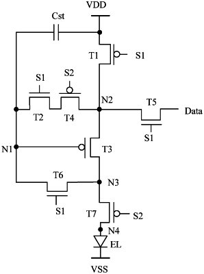
1. A pixel circuit, comprising a driving sub-circuit, a writing sub-circuit, a compensation sub-circuit, and a reset sub-circuit, wherein
the driving sub-circuit is connected with a first node, a second node, and a third node respectively, and is configured to provide a driving current to the third node in response to a control signal of the first node;
the writing sub-circuit is connected with a first scan signal line, a data signal line, and the second node respectively, and is configured to write a signal of the data signal line to the second node in response to a control signal of the first scan signal line, wherein the signal of the data signal line is a data voltage signal or a reset voltage signal;
the compensation sub-circuit is connected with a first power supply line, the first scan signal line, the first node, and the third node respectively, and is configured to write the reset voltage signal to the third node in response to the control signal of the first scan signal line; the compensation sub-circuit is further configured to compensate the first node in response to the control signal of the first scan signal line;
the reset sub-circuit is connected with the first scan signal line, a second scan signal line, the first node, and the second node respectively, and is configured to write the reset voltage signal to the first node in response to control signals of the first scan signal line and the second scan signal line;
the pixel circuit further comprises a first light-emitting control sub-circuit and a second light-emitting control sub-circuit;
the first light-emitting control sub-circuit is connected with the first power supply line, the first scan signal line, and the second node respectively, and is configured to provide a signal of the first power supply line to the second node in response to the control signal of the first scan signal line; and
the second light-emitting control sub-circuit is connected with the second scan signal line, the third node, and a fourth node respectively, and is configured to write the reset voltage signal to the fourth node in response to the control signal of the second scan signal line; and the second light-emitting control sub-circuit is further configured to allow a driving current to pass between the third node and the fourth node.
|