| CPC G09G 3/32 (2013.01) [G09G 3/2007 (2013.01); H01L 25/167 (2013.01)] | 20 Claims |
|
1. A pixel comprising:
a light-emitting element;
a first transistor connected between a first power source line, which is configured to provide a first power source voltage, and a first node, and configured to generate a drive current flowing from the first power source line to a second power source line, which is configured to provide a second power source voltage, through the light-emitting element;
a second transistor connected between a third power source line, which is configured to provide a reference voltage, and a gate electrode of the first transistor;
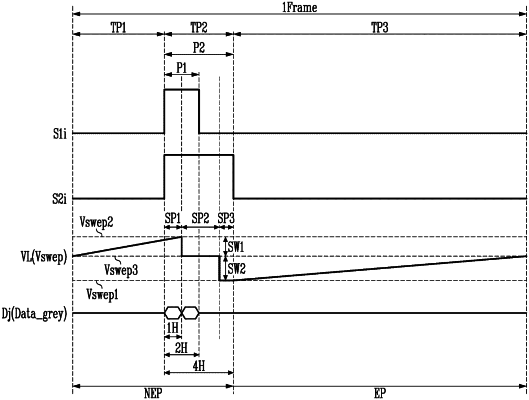
a third transistor connected between a data line, which is configured to provide a grayscale voltage, and a gate electrode of the second transistor, and configured to be turned on in response to a first scan signal;
a fourth transistor connected between a fourth power source line, which is configured to provide a sensing voltage, and the first node, and configured to be turned on in response to a second scan signal;
a first capacitor between the gate electrode of the first transistor and the first node; and
a second capacitor between the gate electrode of the second transistor and a sweep voltage line, which is configured to provide a sweep voltage that linearly changes from a first voltage level to a second voltage level in response to a control signal, and that nonlinearly changes from the second voltage level to a third voltage level during a period in which the grayscale voltage is provided by the third transistor to the gate electrode of the second transistor.
|