| CPC G09G 3/2007 (2013.01) [G09G 3/3225 (2013.01); G09G 3/3233 (2013.01); G09G 3/3258 (2013.01); H10K 59/131 (2023.02); G09G 2300/0408 (2013.01); G09G 2300/0426 (2013.01); G09G 2300/0819 (2013.01); G09G 2300/0842 (2013.01); G09G 2300/0852 (2013.01); G09G 2300/0861 (2013.01); G09G 2310/0254 (2013.01); G09G 2310/061 (2013.01); G09G 2310/08 (2013.01); G09G 2320/0233 (2013.01); G09G 2320/0247 (2013.01); G09G 2320/0252 (2013.01); G09G 2320/0257 (2013.01); G09G 2320/045 (2013.01); G09G 2320/0626 (2013.01)] | 18 Claims |
|
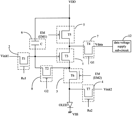
1. A pixel driving circuit, comprising: a data writing sub-circuit, a threshold compensation sub-circuit, a driving sub-circuit, a storage sub-circuit and a data voltage supply sub-circuit, wherein
the data writing sub-circuit comprises a fourth transistor, a first electrode of the fourth transistor is connected with a data line, a second electrode of the fourth transistor is connected with a first terminal of the driving sub-circuit, and a control electrode of the fourth transistor is connected with a first scan signal line, and the fourth transistor is an oxide thin film transistor;
the threshold compensation sub-circuit is configured to compensate a threshold voltage of the driving sub-circuit in response to a second scan signal;
the storage sub-circuit is configured to store a data voltage signal plus a threshold voltage of the driving sub-circuit;
the driving sub-circuit is configured to provide a driving current for a light emitting device to be driven according to voltages of the first terminal and a control terminal of the driving sub-circuit; and
the data voltage supply sub-circuit is configured to write a first voltage into the data line in an initialization stage, so that the data writing sub-circuit transmits the first voltage to the first terminal of the driving sub-circuit; the first voltage is greater than or equal to a data voltage corresponding to a maximum brightness value that the light emitting device displays; or, the first voltage is greater than or equal to a data voltage corresponding to a minimum brightness value that the light emitting device displays.
|