| CPC G09G 3/2007 (2013.01) [G09G 3/3225 (2013.01); G09G 3/3233 (2013.01); G09G 3/3258 (2013.01); H10K 59/131 (2023.02); G09G 2300/0408 (2013.01); G09G 2300/0426 (2013.01); G09G 2300/0819 (2013.01); G09G 2300/0842 (2013.01); G09G 2300/0852 (2013.01); G09G 2300/0861 (2013.01); G09G 2310/0254 (2013.01); G09G 2310/061 (2013.01); G09G 2310/08 (2013.01); G09G 2320/0233 (2013.01); G09G 2320/0247 (2013.01); G09G 2320/0252 (2013.01); G09G 2320/0257 (2013.01); G09G 2320/045 (2013.01); G09G 2320/0626 (2013.01)] | 16 Claims |
|
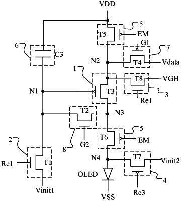
1. A pixel driving circuit, comprising:
a driving circuit, coupled to a first node and a second node, and configured to output a driving current according to a voltage difference between the first node and the second node;
a first reset circuit, coupled to the first node, a first initial signal terminal and a first reset signal terminal, and configured to transmit a signal of the first initial signal terminal to the first node in response to a signal of the first reset signal terminal; and
a second reset circuit, coupled to the second node and a first power terminal, and configured to transmit a signal of the first power terminal to the second node in response to a control signal,
wherein a turn-on level of the second reset circuit and a turn-on level of the first reset circuit have opposite polarities;
the second reset circuit is further coupled to a second reset signal terminal, and is configured to transmit the signal of the first power terminal to the second node in response to a signal of the second reset signal terminal; and
wherein the signal of the second reset signal terminal and the signal of the first reset signal terminal have opposite polarities.
|