| CPC G09G 3/006 (2013.01) [H01L 27/124 (2013.01); G09G 2300/0443 (2013.01); G09G 2300/0452 (2013.01); G09G 2330/12 (2013.01)] | 20 Claims |
|
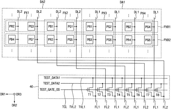
1. A display device comprising:
a first pixel row including a first first-color sub-pixel and a second first-color sub-pixel both configured to display a first color;
a first first-structure transmission line;
a first second-structure transmission line neighboring the first first-structure transmission line with no intervening transmission line disposed in a display panel test circuit and connected to a sub-pixel which displays a different color than the first color;
a first transistor electrically connected through the first first-structure transmission line to the first first-color sub-pixel and configured to receive a first test voltage; and
a second transistor electrically connected through the first second-structure transmission line to the second first-color sub-pixel and configured to receive a second test voltage different from the first test voltage,
wherein the first transistor and the second transistor are disposed in a non-display area of the display device.
|