| CPC G06V 10/147 (2022.01) [G06F 18/243 (2023.01); G06T 5/70 (2024.01); G06T 7/20 (2013.01); G06T 7/70 (2017.01); G06V 10/22 (2022.01); G06V 10/25 (2022.01); H04N 23/667 (2023.01); H04N 23/80 (2023.01)] | 20 Claims |
|
1. A dynamic vision sensor, comprising:
a pixel array comprising a plurality of pixels arranged in a matrix, each pixel configured to generate one or more electrical signals in response to a change in intensity of incident light;
an event detection circuit configured to process electrical signals received from the pixel array, and generate event signals, each event signal of the event signals including a polarity and an address corresponding to a separate electrical signal of the electrical signals;
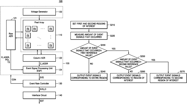
an event rate controller configured to count the event signals and transmit some of the event signals as output event signals in response to a count value of the event signals being equal to or greater than a reference value; and
an interface circuit configured to output the output event signals to an external device,
wherein the event detection circuit includes an address event representation to generate the address.
|