| CPC G06T 7/0008 (2013.01) [G01N 1/32 (2013.01); G06T 7/90 (2017.01); G06T 2207/20081 (2013.01); G06T 2207/20084 (2013.01); G06T 2207/30148 (2013.01)] | 20 Claims |
|
1. A system for delayering integrated circuits (ICs), comprising an optical sensor and a controller, the controller comprising a processor, a memory comprising an optical end-point (OE) module, and communications circuitry;
wherein:
the communications circuitry is configured to communicatively couple with delayering equipment that is configured to perform a delayering process on an IC;
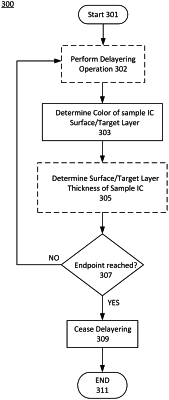
the sensor is configured to image a surface of an IC during or after execution the delayering process by said delayering equipment, and to transmit a sensor signal indicative of a color of a surface layer of the IC to said controller;
in response to said sensor signal, the OE module is configured to cause the controller to:
determine the color of the surface layer of the IC;
determine a thickness of the surface layer of the IC based at least in part on the determined color; and
determine whether an end-point of said delayering process has been reached based at least in part on the determined thickness.
|